PCB Process Explained: What Are Semi-Additive & Subtractive?
PCB Process Explained: What is Semi-Additive & Subtractive?
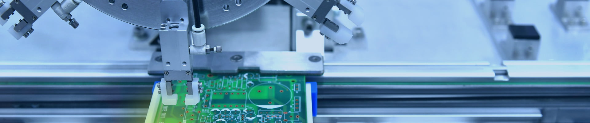
The modern PCB process (including IC substrates) mainly includes Subtractive, Full Additive Process (FAP), and Semi-additive Process (Modified Semi Additive Process, mSAP).
Subtractive
The subtractive PCB process is a method of selectively removing part of the copper foil on the surface of the copper-clad laminate to obtain a conductive pattern. The subtractive is the main process of printed circuit manufacturing today, and its biggest advantage is that the process is mature, stable, and reliable.

Printed circuits manufactured by the subtractive can be divided into the following two categories.
Non-plating-through-hole PCB
This type of printed board is produced by screen printing and then etching the printed board, and it can also be produced by the photochemical process. Non-perforated plated printed boards are mainly single-sided, and there are also a small number of double-sided boards, which are mainly used for televisions and radios.
Plating-through-hole PCB
Use processes such as electroless plating and electroplating on the copper-clad laminate that has been drilled to make the holes between two or more layers of conductive patterns from electrical insulation to electrical insulation. Electrical connections, such printed boards are called perforated plated printed boards. Perforated plated printed boards are mainly used in computers, program-controlled switches, mobile phones, etc.
The different electroplating processes, it is divided into graphic electroplating and full plate electroplating.
(1) Pattern Plating: On the double-sided copper-clad laminate, a conductive pattern is formed by screen printing or photochemical processes, and lead-tin, tin-cerium, tin-nickel, gold, etc. are plated on the conductive pattern. The metal is resisted, and then the resist other than the circuit pattern is removed, and it is etched. The pattern plating process is further divided into a pattern plating and etching (Pattern Plating And Etching) and a bare copper-clad solder mask process (Solder Mask On Bare Copper, SMOBC).
(2) Full-board plating (Panel Plating): On the double-sided copper-clad laminate, copper is electroplated to a specified thickness, and then image transfer is performed by screen printing or photochemical processes to obtain a corrosion-resistant positive-phase circuit image. Remove the resist to make a printed board.
The full plate electroplating can be further subdivided into the via plugging and via tenting.
The advantages of the above process are that the process is simple and the thickness uniformity of the coating layer is good. The disadvantage is that it wastes energy, and it is difficult to manufacture through-hole printed boards without land.
Application of subtractive
The subtractive is the earliest and more mature circuit board manufacturing process. Generally, it refers to the photochemical process, screen printing pattern transfer or electroplating pattern resist layer on the copper clad plate, and then a chemical solution is used to etch away the copper foil of the non-pattern part, or mechanically remove the unnecessary part to make a printed circuit board.
However, in the chemical solution etching process, the etching process is not carried out vertically downward from the surface but is simultaneously etched to both sides of the channel, that is, there is a phenomenon of side etching, which causes the bottom width of the etching channel to be larger than the top.
Due to the existence of side etching, the application of the subtractive in fine-circuit fabrication is greatly limited. When the line width/line spacing requirement is less than 2 mil, the subtractive circuit board process cannot be applied due to the low yield.
At present, the subtractive is mainly used to produce regular PCB, FPC, HDI, and other printed circuit board products.
Additive
Full additive process
The full additive PCB process refers to the process of electroless copper plating after printing a circuit on an insulating substrate containing a photocatalyst without copper cladding.
The copper circuit pattern is plated on the substrate to form a printed circuit board with an electroless copper plating layer as the circuit. Since the circuit is added to the printed circuit board later, it is called additive manufacturing.
The full-additive PCB process is more suitable for making fine circuits, but because it has special requirements for the substrate and chemical immersion copper, and also has strict requirements on the bonding force between the copper plating and the substrate, it is quite different from the traditional PCB manufacturing process. The cost is high and the circuit board process is not mature, and the current output is not large.
The full additive process can be used to produce WB or FC flip chip substrates, and its process can reach below 10μm.
Semi-additive

The semi-additive PCB process refers to covering the photoresist (D/F) on the substrate pre-plated with thin copper and then developing it after exposure, then using electroplating to thicken the copper thickness of the formal traces, remove the photoresist, and then remove the excess copper layer under the photoresist through flash etching.
The characteristic of the semi-additive process is that the formation of the circuit mainly depends on electroplating and flash etching. In the flash etching process, since the etched chemical copper layer is very thin, the etching time is very short, and the lateral etching of the line is relatively small.
Compared with the subtractive, the width of the line will not be affected by the thickness of the electroplated copper, which is easier to control and has a higher resolution. The line width and line spacing of the fine line are almost the same, which can greatly improve the yield of the fine line.
The semi-additive process is currently the main process for producing fine circuits. The mass production capacity can reach a minimum line width/line spacing of 14μm/14μm and a minimum aperture of 55μm. It is widely used in CSP, WB, and FC flip chip substrates and other fine-circuit substrates.
Advantages of additive manufacturing processing
(1) Since the additive avoids a large amount of etching copper and the resulting large amount of etching solution processing costs, the production of printed boards is greatly reduced cost.
(2) Compared with the subtractive, the process of the additive is reduced by about 1/3, which simplifies the PCB production process and improves production efficiency. In particular, the vicious circle of the higher the product grade and the more complicated the process is avoided.
(3) The additive can achieve flush wires and flush surfaces so that SMT and other high-precision printed boards can be manufactured.
(4) In the additive, due to the simultaneous chemical copper plating on the hole wall and the wire, the thickness of the copper plating layer on the hole wall and the conductive pattern on the board surface is uniform, which improves the reliability of the metalized hole and can also meet the requirements of high thickness. Diameter ratio printed board, copper plating requirements in small holes.
Classification of additive
The additive PCB production process of printed boards can be divided into the following three categories:
(1) Full Additive Process, an additive process that only uses chemical copper deposition to form conductive patterns. The process uses catalytic laminates as substrates.
(2) Semi Additive Process, an additive process in which a conductive pattern is formed by chemically depositing metal on the surface of an insulating substrate, combining electroplating etching, or using the three together. The substrate used in the manufacture is a common laminate.
(3) Partial Additive Process, use the additive process to manufacture printed boards on catalytic copper clad laminates.
Semi-Additive or Subtraction?
The comparison of the different processes of PCB and the preliminary exploration of the similar carrier technology are as follows:
Subtractive
Advantage:
1. It can directly make copper-free holes on the large copper skin (no need for two drills) and larger copper-free holes;
2. It can make printed circuit boards with a large residual copper rate on both sides of the outer layer;
3. The process is short and the cost is relatively low.
Disadvantage:
1. It is impossible to make large copper holes and larger copper holes without welding rings, wedding rings, and holes;
2. It is not suitable to make printed circuit boards with high hole copper and thick surface copper (the surface copper is thicker and not easy to be etched);
Semi-additive
Advantage:
1. It can make large copper holes and larger copper holes without welding rings, wedding rings, and holes;
2. Able to make printed circuit boards with high aspect ratio and thick hole copper and thick surface copper (etching only needs to etch the bottom copper and one copper).
Disadvantage:
1. It is impossible to make larger copper-free holes;
2. It is not advisable to make printed circuit boards with large residual copper rates on both sides (due to uneven current distribution during copper electroplating, filming is likely to occur);
3. The process is relatively long and the cost is relatively high.
Technology trend

Currently, the mainstream advanced HDI boards in mobile phone motherboards are manufactured by the subtractive PCB process. After upgrading to a similar substrate, due to the process The requirement is 30/30 microns, so the subtractive will no longer be used, and the mSAP semi-additive needs to be used, similar to the IC carrier board.
From the subtractive of HDI to the semi-additive of mSAP like carrier board SLP, more copper plating processes are designed in the process, and the required copper plating capacity is greatly increased, and for exposure equipment (more complex process) and lamination, The demand for equipment (increased number of product layers) has also increased.
At present, the main players involved in the production capacity preparation of similar substrate include advanced HDI manufacturers and IC substrate manufacturers.
For HDI manufacturers, since the circuit board process is upgraded from the subtractive to the mSAP semi-additive, new equipment investment is required, and the learning curve of yield ramping is required.
For IC carrier board manufacturers, since the production of the carrier board itself adopts the mSAP PCB process, there is no obstacle in the production of the carrier board in terms of technology and yield, but the requirements for the fineness of the lines of the carrier board are not as high as that of the IC carrier board.
The requirements for equipment are also relatively loose, so IC substrate manufacturers may face the risk of declining profit margins when they switch to the production of similar substrates.
On the whole, in the competitive landscape of similar substrates, HDI circuit board manufacturers are temporarily at a disadvantage in terms of technology and yield but may have advantages in cost, while IC substrate manufacturers have no problems in technology and yield, but in cost control In bad situations.